AD537
REV. C
7
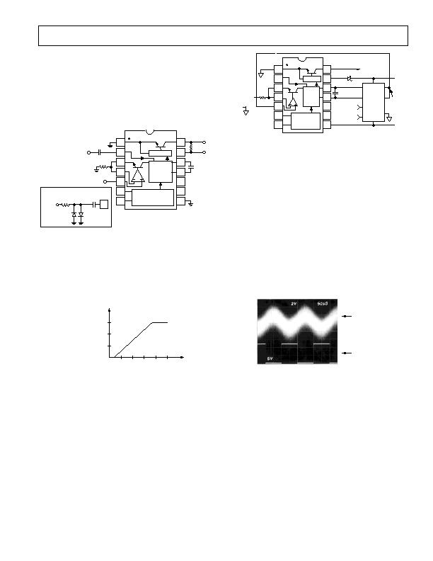
SYNCHRONOUS OPERATION
The SYNC terminal at pin 2 of the DIP package can be used to
synchronize a free running AD537 to a master oscillator, either
at a multiple or a sub-multiple of the primary frequency. The
preferred connection is shown in Figure 10. The diodes are used
to produce the proper drive magnitude from high level signals.
The SYNC terminal can also be used to shut off the oscillator.
Shorting the terminal to +V
S
will stop the oscillator, and the
output will go high (output NPN off).
1
2
14
13
5
6
7
10
9
8
3
4
12
11
AD537
R
+V
S
C
T
f
OUT
V
IN
C
S
V
SYNC
1000pF
2
C
S
V
SYNC
1N4148
10k
NOTE: IF V
SYNC
>2V p-p
USE THIS LIMITER
BUF
DRIVER
CURR-
TO-FREQ
CONV
PRECISION
VOLTAGE
REFERENCE
V
T
V
R
Figure 10. Connection for Synchronous Operation
Figure 11 shows the maximum pull-in range available at a given
signal level; the optimum signal is a 0.8 to 1.0 volt square wave;
signals below 0.1 volt will have no effect; signals above 2 volts
p-p will disable the oscillator. The AD537 can normally be syn-
chronized to a signal which forces it to a higher frequency up to
30% above the nominal free-running frequency, it can only be
brought down about 12%.
0.2 0.4 0.6 0.8 1.0
V
SYNC
SQUARE-WAVE INPUT VOLTS p-p
30%
20%
10%
FREQUENCY
LOCK-IN
RANGE
Figure 11. Maximum Frequency Lock-ln Range vs.
Sync Signal
LINEAR PHASE LOCKED LOOP
The phase-locked-loop F/V circuit described earlier operates
from an essentially noise-free binary input. PLLs are also used
to extract frequency information from a noisy analog signal. To
do this, the digital phase-comparator must be replaced by a lin-
ear multiplier. In the implementation shown in Figure 12, the
triangular waveform appearing across the timing capacitor is
used as one of the multiplier inputs; the signal provides the
other input. It can be shown that the mean value of the multi-
plier output is zero when the two signals are in quadrature. In
this condition, the ripple in the error signal is also quite small.
Thus, the voltage at Pin 5 is essentially zero, and the frequency
is determined primarily by the current in the timing resistor,
controlled either manually or by a control voltage.
1
2
14
13
5
6
7
10
9
8
3
4
12
11
AD537
CAP
0.01礔
OUTPUT
+V
S
V
OS
V
S
SIGNAL
INPUT
?SPAN class="pst AD537SD_2632449_6">12V PK
1
2
6
7
8
10
12
11
14
+15V
COM-
POSITE
ERROR
SIGNAL
?SPAN class="pst AD537SD_2632449_6">1V PK
15V
10k
DEC/
SYN
FREQ
CONTROL
INPUT
0 TO 10V
V
TEMP
V
REF
RECOVERED
FREQUENCY
SIGNAL
3.9V
DRIVER
PRECISION
VOLTAGE
REFERENCE
CURR
-TO-
FREQ
CONV
BUF
LOGIC
GND
V
R
V
T
Figure 12. Linear Phase-Locked Loop
Noise on the input signal affects the loop operation only slightly;
it appears as noise in the timing current, but this is averaged out
by the timing capacitor. On the other hand, if the input fre-
quency changes there is a net error voltage at Pin 5 which acts
to bring the oscillator back into quadrature. Thus, the output at
Pin 14 is a noise-free square-wave having exactly the same fre-
quency as the input signal. The effectiveness of this circuit can
be judged from Figure 13 which shows the response to an input
of 1V rms 1kHz sinusoid plus 1V rms Gaussian noise. The
positive supply to the AD537 is reduced by about 4V in order
to keep the voltages at Pins 11 and 12 within the common-mode
range of the AD534.
Since this is also a first-order loop the circuit possesses a very
wide capture range. However, even better noise-integrating
properties can be achieved by adding a filter between the multi-
plier output and the VCO input. Details of suitable filter charac-
teristics can be found in the standard texts on the subject.
1V RMS SIGNAL
+1V RMS NOISE
OUTPUT
Figure 13. Performance of AD537 Linear Phase Locked
Loop
By connecting the multiplier output to the lower end of the tim-
ing resistor and moving the control input to Pin 5, a high resis-
tance frequency-control input is made available. However, due
to the reduced supply voltage, this input cannot exceed +6V.
TRANSDUCER INTERFACE
The AD537 was specifically designed to accept a broad range of
input signals, particularly small voltage signals, which may be
converted directly (unlike many V-F converters which require
signal preconditioning). The 1.00V stable reference output is
also useful in interfacing situations, and the high input resis-
tance allows nonloading interfacing from a source of varying
resistance, such as the slider of a potentiometer.
发布紧急采购,3分钟左右您将得到回复。
相关PDF资料
AD636JD
IC TRUE RMS/DC CONV MONO 14-CDIP
AD650SD
IC V-F/F-V CONV 1MHZ 14-CDIP
AD652SQ
IC V-F CONV SYNCH MONO 5V 16CDIP
AD654JNZ/+
IC CONV VOLT-FREQ 500KHZ 8DIP
AD7740YRM
IC CONVERTER V TO FREQ 8-MSOP
ADM1070ARTZ-REEL7
IC CTRLR HOTSWAP -48V SOT23-6
ADM1073ARU-REEL
IC CTRLR HOTSWAP -48V 14TSSOP
ADM4210-2AUJZ-RL7
IC CTLR HOTSWAP LV TSOT23-6
相关代理商/技术参数
AD537SD/883B
功能描述:电压频率转换及频率电压转换 IC MONO V/F CONVERTER IC RoHS:否 制造商:Texas Instruments 全标度频率:4000 KHz 线性误差:+/- 1 % FSR 电源电压-最大: 电源电压-最小: 最大工作温度:+ 85 C 最小工作温度:- 25 C 安装风格:Through Hole 封装 / 箱体:PDIP-14 封装:Tube
AD537SH
功能描述:IC V/F CONV TO100-10 RoHS:否 类别:集成电路 (IC) >> PMIC - V/F 和 F/V 转换器 系列:- 标准包装:1 系列:- 类型:频率至电压 频率 - 最大:10kHz 全量程:- 线性:±0.3% 安装类型:表面贴装 封装/外壳:8-SOIC(0.154",3.90mm 宽) 供应商设备封装:8-SOIC 包装:Digi-Reel® 其它名称:LM2917MX-8/NOPBDKR
AD537SH/883B
功能描述:电压频率转换及频率电压转换 IC MONO V/F CONVERTER IC RoHS:否 制造商:Texas Instruments 全标度频率:4000 KHz 线性误差:+/- 1 % FSR 电源电压-最大: 电源电压-最小: 最大工作温度:+ 85 C 最小工作温度:- 25 C 安装风格:Through Hole 封装 / 箱体:PDIP-14 封装:Tube
AD5380BST-3
制造商:Analog Devices 功能描述:DAC 40-CH Resistor-String 14-bit 100-Pin LQFP 制造商:Rochester Electronics LLC 功能描述:32/40-CHANNEL 3V/5V SINGLE SUPPLY 12/14-BIT VOUT DAC - Bulk
AD5380BST-3-REEL
制造商:Analog Devices 功能描述:DAC 40-CH Resistor-String 14-bit 100-Pin LQFP T/R
AD5380BST-5
制造商:Analog Devices 功能描述:DAC 40-CH Resistor-String 14-bit 100-Pin LQFP 制造商:Rochester Electronics LLC 功能描述:40-CHN 5V SINGLE SUPPLY 14-BIT VOUT I.C. - Bulk
AD5380BST-5-REEL
制造商:Analog Devices 功能描述:DAC 40-CH Resistor-String 14-bit 100-Pin LQFP T/R
AD5380BST-U2
制造商:Analog Devices 功能描述:DAC 40-CH RES-STRING 14BIT 100LQFP - Bulk